


If semiconductor technology makes computers work, why does the same word appear on a recovery sleeve? The missing distinction is between what a material does, what an engineered device does, and what a finished product has been shown to achieve. Those aren't interchangeable claims.
Understanding that distinction makes electronics less mysterious and wearable marketing easier to evaluate. You don't need an engineering degree, just a clear map from material to function to evidence.
Table of Contents
- What Semiconductor Technology Means
- How Engineers Control Current in a Semiconductor
- Materials and Device Types Compared
- How Semiconductors Scaled From Lab to Everyday Life
- How Semiconductor Materials Show Up in Recovery Wear
- What the Evidence Supports for Joint Pain
- Decide Whether Semiconductor Recovery Wear Fits Your Routine
What Semiconductor Technology Means
Think of electrical charge moving through a material as water moving through plumbing. A conductor resembles an open pipe, an insulator resembles a sealed barrier, and a semiconductor resembles a valve whose behavior engineers can control.
Semiconductor technology is the practice of making and using materials with electrical conductivity between conductors and insulators, then shaping them into useful electronic devices. Those devices can switch, sense, store, or amplify electrical signals. The important feature isn't intermediate conductivity, but the ability to change it deliberately.
Conductors, semiconductors and insulators compared
| Material class | Example | How it handles charge | Everyday role |
|---|---|---|---|
| Conductor | Copper | Lets charge move freely | Wiring and cables |
| Semiconductor | Silicon | Conducts under conditions controlled by voltage, light, heat or impurities | Switches and processor chips |
| Insulator | Glass | Blocks charge almost completely | Glass-fibre electrical insulation and window panes |
The pipe analogy has limits. A semiconductor isn't a mechanical valve, and charge doesn't move through a crystal exactly as water moves through a hose. But the comparison captures why engineers use these materials: they can build a controllable path rather than a permanently open connection.
From a material to a useful function
Consider a phone's light-sensitive screen adjustment. A sensing element responds to incoming light, a circuit interprets its signal, and other electronics adjust the display. Different components do different jobs, even though semiconductor technology helps make the whole sequence possible.
That's why semiconductor isn't a product category. Silicon is a material; a transistor is a device; a processor combines devices into a circuit; and a phone combines circuits with a battery, screen, software, and other parts.
Practical rule: Ask what property is being controlled and what useful function that control produces.
A useful first question is whether voltage, light, heat, or added impurities change how charge moves through the material. That points toward semiconductor behavior, but it isn't a complete identification test. Ordinary conductors also change resistance with temperature, so a material name and measured electrical behavior matter more than a broad description such as heat activated.
When someone asks, “What is semiconductor technology?”, the clearest answer therefore includes both halves: a controllable material and an engineered function.
How Engineers Control Current in a Semiconductor
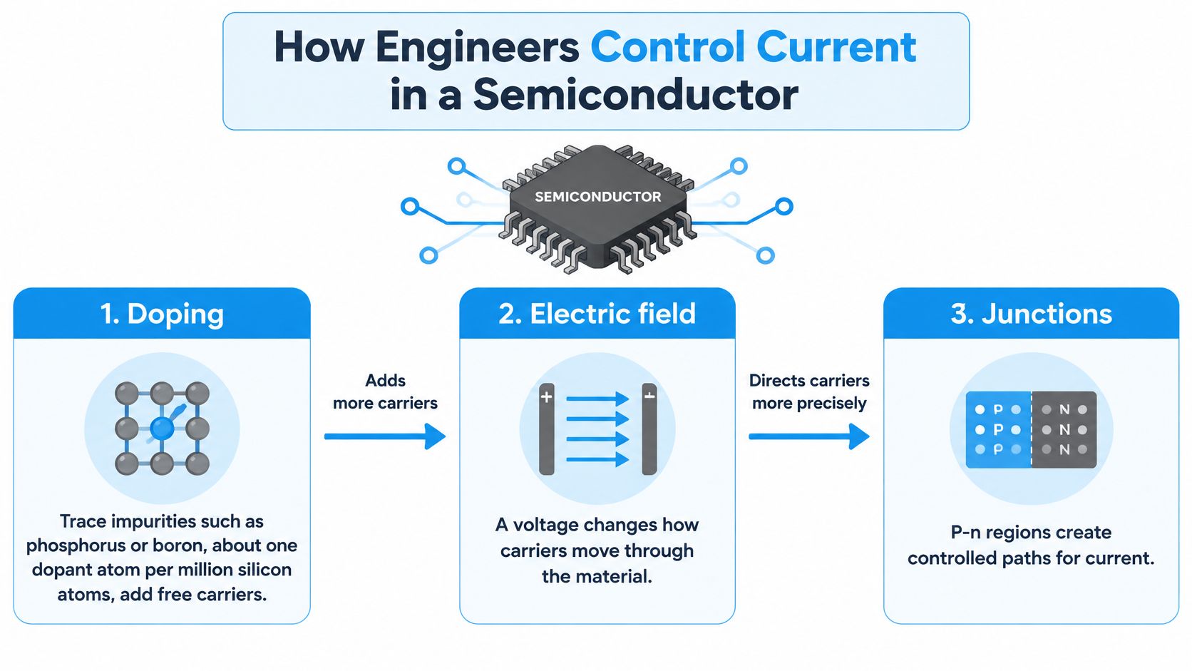
Engineers control semiconductor behavior by changing the available charge carriers, the forces acting on them, and their thermal conditions. The diagram introduces doping, electric fields, and junctions, the boundaries where differently treated semiconductor regions meet.
Doping changes the available carriers
Doping means deliberately introducing small amounts of another element into a semiconductor crystal. In silicon, phosphorus can supply additional electrons, producing n-type material. Boron can create electron vacancies called holes, producing p-type material.
A hole isn't a separate particle inserted into the crystal. It's a missing electron position that can behave like a moving positive charge as neighboring electrons change places. Joining p-type and n-type regions creates a junction, which helps engineers control the direction and conditions of current flow.
Electric fields control the path
In a field-effect transistor, voltage applied to a gate changes the availability of carriers in a narrow channel. The gate can make that channel conductive or resistive without a moving mechanical contact.
A transistor can therefore act as a switch. Digital circuits interpret its electrical states as binary values, commonly described as on and off, although a complete logic circuit determines which state represents which value.
Temperature changes the operating conditions
Heat can free additional charge carriers, while also affecting how easily they travel through the crystal. Engineers account for both effects when designing a device, rather than assuming that warmer always means more useful current.
The defining advantage is controllability through impurities, electric fields, and temperature; Britannica's history of the semiconductor revolution also dates the transistor's invention at Bell Labs to 1947, crediting John Bardeen, Walter Brattain, and William Shockley.
The same principles support different functions. A diode favors current in one direction, while a light or temperature sensor produces an electrical response to its surroundings.
This video provides another way to visualize semiconductor operation.
Keep the control sequence simple:
- Doping sets the carriers: Engineers establish which charges are available.
- The gate controls the channel: An electric field changes the conductive path.
- Temperature changes behavior: Thermal conditions affect carrier availability and movement.
Materials and Device Types Compared
Semiconductor materials and their typical uses
| Material | Typical uses | Notable property |
|---|---|---|
| Silicon | Processors, memory and most integrated circuits | Abundant, highly purifiable, with a useful stable insulating oxide |
| Germanium | Early transistors, infrared optics, some sensors | Higher carrier mobility and lower heat tolerance than silicon |
| Silicon carbide | Power electronics, electric vehicle inverters | Wide bandgap suited to high voltage and temperature |
| III-V compounds, including gallium arsenide and gallium nitride | Radio-frequency amplifiers, LEDs, lasers | Selected compounds support fast electronic operation or light emission |
These materials aren't interchangeable ingredients. Engineers choose them for the electrical, thermal, or optical demands of a particular job. A material suited to controlling an electric vehicle's power supply isn't automatically the best choice for a camera sensor or a memory circuit.
III-V compounds combine elements from different groups of the periodic table. The family includes materials with distinct capabilities, so the table shouldn't be read as saying that every compound performs every listed function equally well.
Classify the device by its job
The federal definition of semiconductors and semiconductor manufacturing encompasses devices and systems with functions including processing, memory, sensing, communications, power conversion, and photonics. That breadth explains why calling every semiconductor a tiny computer is misleading.
A practical function map looks like this:
- Transistors and logic: Switch or amplify signals and implement electronic decisions.
- Diodes: Control current direction or perform specialized electrical and optical functions.
- Memory: Retains information for later use.
- Processors: Execute operations using interconnected logic and supporting circuitry.
- Sensors: Convert a physical input into a usable signal.
- Power-control components: Switch, convert, or regulate electrical power.
- Photonics: Generate, detect, or manipulate light.
An analog component, for example, may handle a continuously changing sensor signal rather than execute software. A power device may regulate energy without storing your photographs or running an application.
Manufacturing is another distinction
Making an integrated circuit involves patterned manufacturing steps such as lithography, deposition, and etching. Engineers define regions, add layers, and remove selected material to construct a working device.
Adding a mineral to a textile isn't automatically equivalent to that process. The mineral might have a useful physical property, but a fabric containing it doesn't thereby contain a processor, memory, or powered sensor.
The same caution applies to familiar material names. Our discussion of copper and therapeutic claims addresses the broader distinction between naming an ingredient and demonstrating a benefit.
Look for both the material name and its assigned function. Silicon carbide used for power conversion tells you something specific. An advanced semiconductor label without an identified task tells you much less.
How Semiconductors Scaled From Lab to Everyday Life
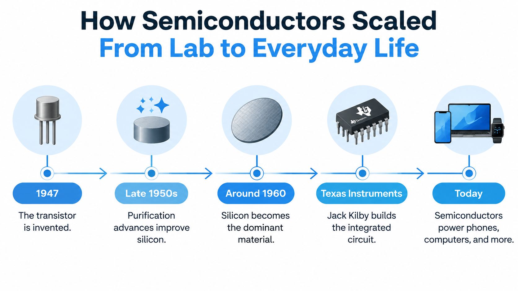
Early transistor engineers worked with germanium before improved purification made silicon commercially practical. The decisive manufacturing change was integration: instead of assembling every electronic function from separately wired components, manufacturers could fabricate interconnected devices together.
That change reduced the assembly work required for increasingly complex circuits. It also made reliability, repeatability, and manufacturing yield central engineering concerns.
The timeline gives a broad visual overview; the integrated-circuit milestone belongs to the same transition toward commercial silicon electronics, rather than a separate development after that transition.
More functions in the available space
In 1965, Gordon Moore observed that integrated-circuit component counts had been approximately doubling annually; he revised the expected pace to roughly every two years in 1975, according to Intel's account of Moore's law.
Moore's law is a historical industry trend, not a law of nature. Engineers have to develop the processes, materials, circuit designs, and manufacturing tools that make further integration possible. A smaller device does not emerge just because a calendar advances.
Consider a portable medical monitor. Its designer needs sensing, signal processing, storage, communication, and power management. When manufacturers can integrate more functions into compact components, the designer can make the monitor easier to carry and less demanding to assemble.
That doesn't mean every component should shrink in the same way. Power handling, heat removal, insulation, and connections still impose practical requirements.
Scale depends on manufacturing equipment
Fabrication also depends on machinery that moves and positions materials reliably. For a concrete view of that less-visible engineering layer, Intech Corporation's resource on motion components for semiconductor equipment connects chip production with the mechanical systems supporting it.
The industry's commercial scale is substantial: global semiconductor sales reached $630.5 billion in 2024, the first annual total above $600 billion, according to the Semiconductor Industry Association's state-of-the-industry report.
Smaller electronics can make a wearable possible. They don't establish whether that wearable improves a health outcome.
Compact devices now fit into places where bulky assemblies would be inconvenient, including clothing and body-worn accessories. Discussions of advancements in pain-management technology should still distinguish engineering capability from clinical effectiveness.
How Semiconductor Materials Show Up in Recovery Wear
A garment's semiconductor description can refer to materially different constructions. Start with what is physically present, not with the promised benefit.
Passive fibres versus powered semiconductor devices
| Form | What is in the garment | Power | What semiconductor can mean | What to verify |
|---|---|---|---|---|
| Passive mineral or carbon fibre | Fibre property, no chip | None | Conductivity or infrared response of the material | Material name and an independent lab note |
| Thermally responsive mineral | Material that absorbs and re-radiates body heat | None | Not automatically a silicon circuit | Infrared method and wash-durability test |
| Powered wearable electronics | Sensor, heater or circuit | Battery or wired supply | An actual semiconductor device | Named function, safety listing and failure mode |
The passive categories can overlap. A mineral-containing fibre might have measurable electrical properties and a thermal response, but neither property proves that the garment senses the wearer or actively regulates its temperature.
A powered wearable raises different questions. You need to know what receives power, what it measures or controls, and what happens if its electrical system fails.
Read the mechanism literally
Infrared interaction describes an exchange of electromagnetic energy. It doesn't, by itself, specify how much energy is involved, where it goes, or whether the wearer experiences a meaningful difference.
Likewise, negative-ion release, electrical conductivity, and infrared response are separate measurable properties. Evidence for one shouldn't stand in for testing another.
The illustration introduces textile construction concepts, but its benefit labels should be evaluated separately from its material descriptions.
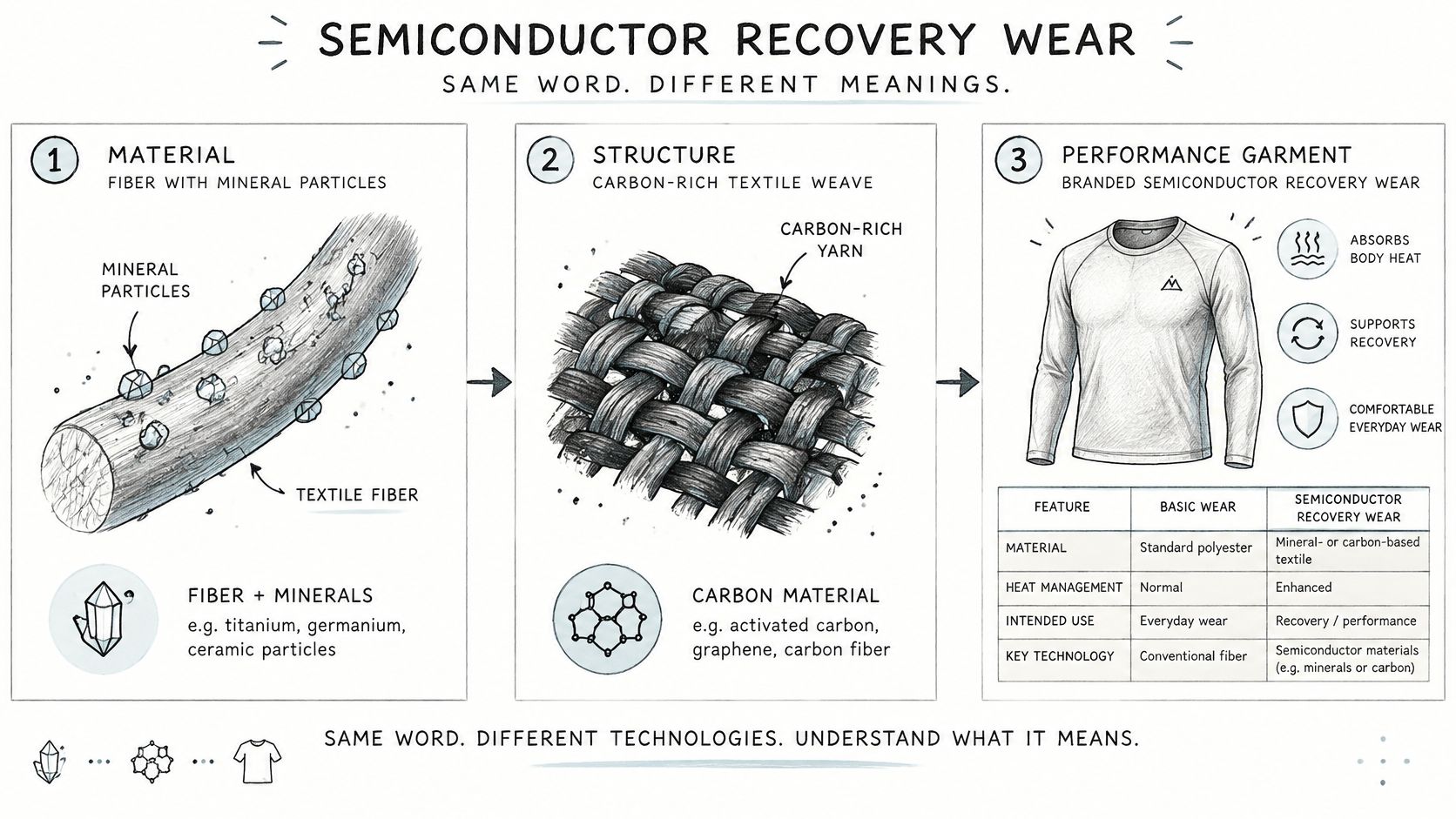
For any garment, useful documentation identifies the fibre or mineral, explains the proposed infrared interaction, and states whether electronics are present. If the description says an ingredient remains effective after laundering, look for testing on washed fabric, not only on an unused material sample.
Our explainer on germanium's role in recovery discussions provides ingredient context. Ingredient context still needs to be distinguished from product-specific measurements and human outcomes.
Separate thermal precautions from material claims
A passive garment and an electrically heated wrap shouldn't be used as though they were identical. For readers comparing those categories, wearable wrap safety tips from SunnyBay offer a practical companion resource for examining heat-wrap use.
Manufacturer descriptions explain the proposed mechanism. Independent measurements establish what the material does under stated conditions. Clinical testing must answer the separate question of what benefit people experience.
What the Evidence Supports for Joint Pain
A material can interact with electromagnetic energy without producing a clinically meaningful improvement in osteoarthritis. A garment can feel warm without outperforming an ordinary sleeve, and a person can report comfort without experiencing improved joint function.
Keep these claims separate:
- Material response: The fibre has a measurable electrical or infrared property.
- Thermal effect: The finished garment changes heat retention or skin temperature.
- Perceived comfort: The wearer notices warmth or reduced stiffness.
- Clinical benefit: Controlled human testing demonstrates an improvement in pain or function.
Industry growth doesn't close the gaps between those claims. The Semiconductor Industry Association's market data reports worldwide semiconductor sales of $791.7 billion in 2025, up 25.6% from the previous year; those are commercial results, not evidence for a recovery garment.
Read the manufacturer claim alongside its limits
At Thermo Recovery Wear, our material descriptions identify bamboo charcoal as a natural semiconductor, distinguish it from regular bamboo fabric, and describe body-heat-activated negative-ion release. We offer germanium-and-carbon products while transitioning toward exclusively recycled and eco-friendly materials; our semiconductor elements are integrated before product manufacture, and we state that they remain permanent and effective through washing. We also report relief of chronic osteoarthritic joint pain by up to 62% from our semiconductor-embedded fabric.
These are manufacturer claims. The pain percentage needs its underlying human study, while the material and laundering statements call for appropriate laboratory reports.
Semiconductor recovery wear claims and the evidence to check
| Claim | What it means | Evidence status | What to check |
|---|---|---|---|
| Fabric responds to infrared energy | Physical property of the fibre | Measurable in a lab setting | Independent test reports and test conditions |
| Garment feels warmer on skin | Warmth from body heat and fabric insulation | Plausible, but subjective without measurement | Compare comfort against an ordinary sleeve |
| Relieves joint pain by up to 62% | Company-reported figure for osteoarthritis pain | Underlying study design isn't shown here | Sample, controls and outcome measured |
| Improves blood flow | A mechanism proposed by the manufacturer | Not established here as a medical outcome | Direct circulation measurements and clinical interpretation |
| Works for all joints and skin types | A broad generalisation | Not established across populations | Which joints and participant groups were actually tested |
Questions that make a percentage useful
Ask whether the reported result was an average, a best result, or a change in a selected subgroup. Check the sample size, comparison group, study independence, duration, and whether participants also changed medication or activity.
Pain, stiffness, and function are different outcomes. A pain score doesn't automatically establish easier walking, better sleep, or improved circulation.
A proposed biological mechanism is a reason to investigate a treatment, not a substitute for testing it.
Our discussion of far-infrared waves and cellular-health claims should be read with that distinction in mind. Mechanical products require a different assessment too: Asterisk Cell braces at Rider 18 illustrate why a brace comparison should examine intended support and fit rather than assume a shared mechanism with thermal textiles.
People with reduced sensation, neuropathy, or circulation disorders should seek clinical advice before using warmth-based garments. Treat recovery wear as an adjunct to care, not a replacement for diagnosis or prescribed treatment.
Decide Whether Semiconductor Recovery Wear Fits Your Routine
Choose according to the garment's actual construction, the evidence behind its claims, and your medical circumstances. A material name shouldn't outweigh fit, skin comfort, or a clear explanation of what the garment is intended to do.
Use this sequence before making it part of your routine.
- Confirm whether anything is powered. Check for a battery, charger, wiring, sensor, or controller. With none present, assess the item as a passive textile rather than an electronic treatment that switches on.
- Match the ingredient to the claimed function. Read the composition and care information together. For a laundering claim, the useful document identifies the washing conditions and compares relevant measurements before and after washing.
- Request the document behind a percentage. Use the evidence criteria above to distinguish a controlled comparison from a testimonial or an unexplained headline. Check whether the measured outcome matches the benefit you want.
- Start cautiously if your skin is sensitive. Sensitive-skin or antimicrobial wording doesn't guarantee personal tolerance. Try a short period on a small area, inspect your skin, and stop if you develop itching, redness, burning, or a rash.
- Get advice before adding warmth when sensation is reduced. Neuropathy and poor circulation can make self-monitoring less reliable. Don't use your ability to tolerate discomfort as the only safety check.
- Coordinate with existing treatment. If you have a diagnosed joint condition or take medicines affecting circulation or skin, ask your clinician how the garment fits your care plan. Don't delay assessment of new swelling, persistent pain, or a changing joint problem.
Use a comfort-based decision rule
Compare the garment with an ordinary sleeve during similar activities and conditions. Note comfort, stiffness, skin response, and whether everyday tasks feel easier, without changing several treatments at once.
Our guide to choosing recovery wear can help organize the practical fit and use questions. Continue only if the garment is comfortable, appropriate for your condition, and useful in your routine.
The decision rule is simple: evaluate it as a comfort adjunct, not as proof that a semiconductor label treats a joint disease.
Thermo Recovery Wear offers compression-lite recovery sleeves and braces made with semiconductor-integrated, infrared-responsive fabrics for rest and light daily activity. Visit Thermo Recovery Wear to compare material options, review sizing and care instructions, and choose a garment with the same attention to construction and evidence you'd give any recovery aid.


